The idea: one memory, one ALU, several short cycles
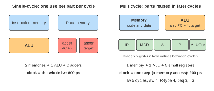
The single-cycle processor runs every instruction in one long clock cycle. It needs two memories (one for instructions, one for data) and two extra adders, because each part can be used only once per cycle. The multicycle processor of Patterson and Hennessy breaks each instruction into steps and runs one step per clock cycle. Then one memory and one ALU are enough: the same ALU adds PC + 4 in one cycle and an address or a sum in a later one.
Press Clock Once to run one clock cycle. The state that runs is orange in the state machine, the wires and muxes it uses turn red, the control signals it sets are orange, and the values move as blue boxes. At the clock edge the registers that were written turn green.
The registers between the steps
A value made in one cycle is needed in the next one, so it must be stored. That is the job of five registers the program cannot see:
| Register | Written in | Holds |
|---|---|---|
IR (instruction register) | state 0 | the instruction word; kept until the next fetch, because IRWrite is 1 only in state 0 |
MDR (memory data register) | state 3 | the word a lw read |
A, B | state 1 | the registers rs and rt |
ALUOut | states 1, 2, 6 | the ALU result: a branch target, an address or a sum |
One memory now holds both the program and the data, so its address must be chosen: the IorD mux picks the PC (to fetch an instruction) or ALUOut (to read or write data). Look at the memory panel: rows 0x00 to 0x20 are code, rows 0x40 to 0x48 are data.
One step per cycle
The rule for a step: it may do at most one memory access, one register file access or one ALU operation. Then the clock period only has to fit the slowest step, not the whole instruction.
- Fetch (state 0):
IR ← Mem[PC], and the ALU computesPC ← PC + 4at the same time. - Decode (state 1):
A ← Reg[rs],B ← Reg[rt], andALUOut ← PC + (sign-extend(imm) << 2). The branch target is computed before the processor knows the instruction is a branch: the ALU is free, and it saves a cycle forbeq. - Execute: an address (state 2), an R-type operation (state 6), a branch compare (state 8) or a jump (state 9).
- Memory:
lwreads (state 3),swwrites (state 5); R-type writes its result (state 7). - Write back:
lwwritesMDRintort(state 4).
The control unit is a finite state machine
In the single-cycle processor the control is a truth table on the opcode. Here the signals must change from cycle to cycle, so the control is a finite state machine: each state sets the signals for one cycle and chooses the next state. States 0 and 1 are the same for all instructions; at the end of state 1 the opcode picks the path.
| State | Does | Signals | Next |
|---|---|---|---|
| 0 fetch | IR ← Mem[PC]; PC ← PC + 4 | MemRead, IRWrite, PCWrite; IorD 0, ALUSrcA 0, ALUSrcB 01, ALUOp 00, PCSource 00 | 1 |
| 1 decode | A, B ← Reg; ALUOut ← branch target | ALUSrcA 0, ALUSrcB 11, ALUOp 00 | lw, sw: 2; R-type: 6; beq: 8; j: 9 |
| 2 address | ALUOut ← A + sign-extend(imm) | ALUSrcA 1, ALUSrcB 10, ALUOp 00 | lw: 3; sw: 5 |
| 3 lw read | MDR ← Mem[ALUOut] | MemRead, IorD 1 | 4 |
| 4 lw write | Reg[rt] ← MDR | RegWrite, RegDst 0, MemtoReg 1 | 0 |
| 5 sw write | Mem[ALUOut] ← B | MemWrite, IorD 1 | 0 |
| 6 execute | ALUOut ← A op B | ALUSrcA 1, ALUSrcB 00, ALUOp 10 | 7 |
| 7 R write | Reg[rd] ← ALUOut | RegWrite, RegDst 1, MemtoReg 0 | 0 |
| 8 branch | if A = B: PC ← ALUOut | ALUSrcA 1, ALUSrcB 00, ALUOp 01, PCWriteCond, PCSource 01 | 0 |
| 9 jump | PC ← {PC[31:28], IR[25:0], 00} | PCWrite, PCSource 10 | 0 |
A signal that a state does not list is 0 if it is a write enable, and don't care (X) if it is a mux select. ALUSrcB picks one of four inputs: 00 = B, 01 = the constant 4, 10 = the sign-extended immediate, 11 = the immediate shifted left by 2. PCSource picks the ALU result (PC + 4), ALUOut (the branch target) or the jump address. The PC is written when PCWrite is 1, or when PCWriteCond is 1 and the ALU's Zero output is 1.
Cycles per instruction
The number of cycles is the length of the instruction's path through the state machine:
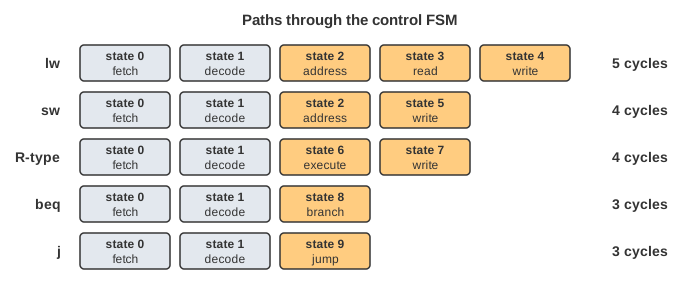
The program on the canvas runs each kind once (Demos 1 to 5): two lw that load 7 and 7, a beq that is taken because they are equal and skips 0x0C, an add that makes 14, a sw that stores it at 0x48, and a j that skips 0x1C and ends the program at 0x20. That is 5 + 5 + 3 + 4 + 4 + 3 = 24 cycles for 6 instructions: CPI = 4.00 (Demo: the whole program). A beq takes 3 cycles whether it is taken or not.
CPI from an instruction mix, and the clock
A real program runs different instructions in different amounts, so its CPI is the average weighted by the instruction mix. Patterson and Hennessy use the SPECint2000 mix: 25% loads, 10% stores, 52% R-type, 11% branches, 2% jumps (Demo: CPI of the textbook mix):
CPI = 0.25 × 5 + 0.10 × 4 + 0.52 × 4 + 0.11 × 3 + 0.02 × 3
    = 1.25 + 0.40 + 2.08 + 0.33 + 0.06 = 4.12
Time per program is instructions × CPI × clock period. Take the book's delays: memory 200 ps, ALU 100 ps, register file 50 ps. The single-cycle clock must fit a whole lw: 200 + 50 + 100 + 200 + 50 = 600 ps. The multicycle clock must fit one step, the longest being a memory access: 200 ps. So one instruction takes 4.12 × 200 = 824 ps on average, against 600 ps. The short clock does not pay off here: a lw needs 5 × 200 = 1,000 ps, and only beq and j (3 × 200 = 600 ps) break even.
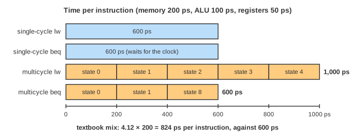
So why build it? It needs less hardware (one memory, one ALU), its steps are a good start for pipelining, which overlaps them, and its control can grow: more states give longer instructions such as multiply (Multiply and Divide Hardware) or the exception states of Exceptions in the MIPS Processor. Register setup and clock-to-Q overheads make the real multicycle clock even longer; Single-Cycle vs Multicycle vs Pipelined MIPS: a Performance Race runs the three designs side by side with Harris and Harris's delays.
See also How a Program Runs on the MIPS Datapath, the five-stage unpipelined datapath of Hennessy and Patterson's Quantitative Approach, with separate instruction and data memories and the NPC, LMD and Cond registers.
What the page leaves out
- In the book,
A,B,MDRandALUOuthave no write enable and load a new value at every clock edge. The page shows only the loads that the next state uses. - Other instructions (
addi,bne, shifts) need more states or more control lines; exceptions add states 10 and 11 and the EPC and Cause registers. - The control can also be built as microprogram ROM words instead of a hard-wired state machine; the states and signals are the same.
- Memory is ideal: every access takes one cycle. A cache miss would stall the state machine for many cycles.
- Only 4 of the 32 registers are shown, and the control lines are drawn as a panel, not as wires from the control unit.
On the mind map
References
Patterson and Hennessy, Computer Organization and Design: The Hardware/Software Interface, 3rd edition, Section 5.5: A Multicycle Implementation (Figures 5.28, 5.37 and 5.38); Section 4.4 of later editions for the single-cycle delays
Harris and Harris, Digital Design and Computer Architecture, Section 7.4: Multicycle Processor