The idea: one instruction per clock cycle
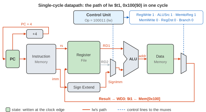
The picture is the complete single-cycle MIPS processor from Harris and Harris, Digital Design and Computer Architecture (Figure 7.11). It runs every instruction in exactly one clock cycle. During the cycle, values flow from the PC through the memories, the register file, the ALU and the muxes, and settle. At the rising clock edge the results are stored: the new PC, one register and one memory word. Then the next instruction starts.
See also Embedded I/O: the same Address, WriteData and MemWrite signals reach I/O device registers through an address decoder (memory-mapped I/O).
See also Memory Arrays: how the register file's two read ports and one write port, and the SRAM and DRAM behind the instruction and data memories, are built from bit cells, wordlines and bitlines.
Press Step Instruction. The cycle is shown in 6 steps so you can follow it, but steps 1 to 5 all happen in the same cycle and change nothing: they are combinational logic settling. Only step 6, the clock edge, writes state (green). Red wires carry a value the instruction uses; faded wires are not used. Blue lines are control signals from the Control Unit; they turn red when asserted (1).
State elements and combinational logic
| Part | Kind | What it does here |
|---|---|---|
PC | state (register, has CLK) | address of the current instruction; loads PC' at the clock edge |
| Instruction Memory | read only, combinational read | RD = Mem[A]: Instr |
| Register File | state (CLK, WE3) | reads RD1 = reg[A1], RD2 = reg[A2] at any time; writes reg[A3] ← WD3 at the edge if WE3 (RegWrite) is 1 |
| Data Memory | state (CLK, WE) | reads ReadData = Mem[A]; writes Mem[A] ← WD at the edge if WE (MemWrite) is 1 |
ALU, two adders, Sign Extend, <<2, 4 muxes, Control Unit, AND gate | combinational | compute SrcA op SrcB, PC + 4, the branch target, and steer values |
The muxes, adders and the ALU are built from gates in Combinational Logic; the registers are edge-triggered flip-flops from Sequential Logic.
How the ALU's adder can be made fast (carry-lookahead and prefix adders), how it subtracts and compares, and how shifts and multiplies are built: Arithmetic Circuits.
The Control Unit: two small truth tables
The Control Unit reads only two fields of the instruction: Op (bits 31:26) and Funct (bits 5:0). The main decoder turns Op into the control lines; the ALU decoder turns ALUOp and Funct into the 3-bit ALUControl. Both tables are drawn on the canvas; the active row is highlighted.
| Instruction | Op | RegWrite | RegDst | ALUSrc | Branch | MemWrite | MemtoReg | ALUOp |
|---|---|---|---|---|---|---|---|---|
| R-type | 000000 | 1 | 1 | 0 | 0 | 0 | 0 | 10 |
lw | 100011 | 1 | 0 | 1 | 0 | 0 | 1 | 00 |
sw | 101011 | 0 | X | 1 | 0 | 1 | X | 00 |
beq | 000100 | 0 | X | 0 | 1 | 0 | X | 01 |
addi | 001000 | 1 | 0 | 1 | 0 | 0 | 0 | 00 |
Each line steers one part of the datapath:
- RegWrite: write enable of the register file (
WE3). - RegDst: which field names the destination register,
rt(bits 20:16, I-type) orrd(bits 15:11, R-type). Its output isWriteReg. - ALUSrc: the second ALU input
SrcBisRD2(a register) orSignImm(the constant). - Branch and the ALU's Zero flag give PCSrc = Branch AND Zero: the next PC is
PCPlus4orPCBranch. - MemWrite: write enable of the data memory (
WE). - MemtoReg: the value written back,
Result, isALUResultorReadDatafrom memory. - ALUOp:
00add (addresses,addi),01subtract (beqcompares),10"look atFunct" (R-type).
X means don't care: sw and beq write no register, so it does not matter what RegDst and MemtoReg select. A hardware designer picks whatever makes the logic smallest; the page fades those lines.
| ALUOp | Funct | ALUControl |
|---|---|---|
| 00 | X | 010 (add) |
| X1 | X | 110 (subtract) |
| 1X | 100000 (add) | 010 (add) |
| 1X | 100010 (sub) | 110 (subtract) |
| 1X | 100100 (and) | 000 (and) |
| 1X | 100101 (or) | 001 (or) |
| 1X | 101010 (slt) | 111 (set less than) |
One instruction of each kind
| Instruction | Path through the datapath | At the clock edge |
|---|---|---|
R-type add $t0, $s0, $s1 | RD1, RD2 → ALU (ALUSrc 0); ALUResult → Result (MemtoReg 0); WriteReg = rd (RegDst 1) | $t0 ← Result, PC ← PC + 4 |
lw $t1, 0x100($0) | RD1 + SignImm → ALU = address; ReadData → Result (MemtoReg 1); WriteReg = rt | $t1 ← Mem[address] |
sw $t0, 0x100($0) | RD1 + SignImm = address; RD2 → WD | Mem[address] ← $t0 (MemWrite 1) |
beq $t2, $0, skip | RD1 − RD2 in the ALU, Zero; PCPlus4 + (SignImm << 2) in the branch adder | PC ← PCBranch if Zero, else PC + 4 |
addi $s0, $0, 5 | RD1 + SignImm; ALUResult → Result; WriteReg = rt | $s0 ← 5 |
Every instruction reads two registers and sign-extends the low 16 bits, whether it needs them or not: the hardware does it in parallel with decoding, so it costs no time. The branch offset counts instructions after the next one, so the target is PCPlus4 + (SignImm << 2): shifting left by 2 multiplies by 4 bytes per instruction. The Instr fields bar under the canvas splits each fetched word into its fields, for example lw $t1, 0x100($0) is 0x8C090100: op 35, rs 0, rt 9, imm 0x100.
The programs
- One of each (Demo):
addi,add,sw,lw,sub, abeqthat is taken and skips an instruction, one that is not taken, andslt. 9 instructions in 9 cycles;mem[0x100] = 17,$s3 = 1. - Array sum: sums 5, 7 and 9. Figure 7.11 has no jump, so the loop goes back with
beq $0, $0, loop, which is always taken. 23 instructions in 23 cycles;mem[0x10C] = 21. - Max of two:
sltandbeqchoose the larger of 12 and 30;mem[0x108] = 30. - Or type an instruction (or pick a sample) and press Execute Instruction: it is written into instruction memory at the current PC and run. Try
add $0, $s0, $s1:RegWriteis 1, but$0stays 0.
Why one cycle is slow
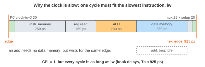
CPI is exactly 1, but the clock period must be long enough for the slowest instruction to settle. That is lw: PC clock-to-Q, instruction memory read, register file read, sign extend and mux, ALU, data memory read, the MemtoReg mux, and the register file setup time:
Tc = tpcq_PC + tmem + max(tRFread, tsext + tmux) + tALU + tmem + tmux + tRFsetup
With the book's example delays (memory 250 ps, ALU 200 ps, register file read 150 ps, ...), Tc is about 925 ps, even though an add or a beq would be done much sooner. It also needs two memories, an extra adder for the branch target, and an ALU that is idle while memory is read.
| Design | Cycles per instruction | Clock period | Page |
|---|---|---|---|
| Single-cycle | 1 | long: the slowest instruction (lw) | this page |
| Multicycle | 3 to 5 | short: one step (one memory access or one ALU operation) | How a Program Runs on the MIPS Datapath |
| Pipelined | about 1 (plus stalls) | short: one stage | The MIPS Pipeline: Hazards and Forwarding |
What the page leaves out
j(jump): Figure 7.11 has no jump path. The book adds one with a third input to the PC mux and aJumpcontrol line.- Other instructions (
orineeds a zero-extender, shifts needshamt), exceptions, and overflow traps onadd. - Only 8 of the 32 registers are shown and accepted, 11 words of instruction memory from address 0 and 8 words of data memory at 0x100–0x11C. Real MIPS starts code at 0x00400000.
- Timing: wires settle instantly here. The steps 1 to 5 are one moment split up for explanation, not real time.
References
Harris and Harris, Digital Design and Computer Architecture, Chapter 7: Microarchitecture (Section 7.3, the single-cycle processor; Figure 7.11, Tables 7.2, 7.3 and 7.5)