What the animation shows
A processor runs a program one instruction at a time: it fetches the instruction the program counter (PC) points at, works out what it asks for, does it, and moves the PC on. The picture above is the datapath that does this in the classic textbook MIPS from Hennessy and Patterson's Computer Architecture: A Quantitative Approach. It is the multicycle, unpipelined version: each instruction takes several clock cycles, one per stage, and the next instruction starts only when the previous one is done. For the simpler design that runs each instruction in one long clock cycle, with its Control Unit drawn, see The Single-Cycle MIPS Processor.
Press Step Cycle to run one clock cycle. The wires that carry a value in that cycle turn red, yellow chips show the values moving, and the registers they write turn green. After the ID stage, the wires the instruction will not use fade out: the opcode has decided which path it takes.
What the names mean
| Name | Stands for | Written in | Holds |
|---|---|---|---|
PC | Program Counter | MEM | the address of the instruction to fetch next |
NPC | Next Program Counter | IF | PC + 4: the next instruction in order. It becomes the new PC in MEM unless a branch is taken, and a branch adds its offset to it in EX. |
IR | Instruction Register | IF | the 32-bit instruction just fetched; its fields drive the rest of the datapath |
A, B | the two register operands | ID | the values of registers rs and rt |
Imm | Immediate (a capital I) | ID | the 16-bit constant inside the instruction, sign-extended to 32 bits: the 42 in addi r5, r0, 42, the 4 in lw r4, 4(r1), or a branch offset |
ALUOutput | ALU output | EX | the ALU's result: a sum or comparison, a memory address, or a branch target |
Cond | Condition | EX | 1 if the branch is taken (from the Zero? test on A), else 0 |
LMD | Load Memory Data | MEM | the word a load (LW) read from data memory, written into a register in WB |
Mux | Multiplexer | picks one of its inputs, set by the control |
The five stages
Every instruction goes through the same first two stages. After that its type decides what happens:
| Stage | All instructions | ALU (ADD, ADDI, ...) | Load (LW) | Store (SW) | Branch (BEQZ, BNEZ) |
|---|---|---|---|---|---|
| IF instruction fetch | IR ← Mem[PC]; NPC ← PC + 4 | ||||
| ID decode / register fetch | A ← Regs[rs]; B ← Regs[rt]; Imm ← sign-extend(imm16) | ||||
| EX execute / address | ALUOutput ← A op B or A op Imm | ALUOutput ← A + Imm (the address) | ALUOutput ← NPC + (Imm << 2); Cond ← (A == 0) | ||
| MEM memory access | PC ← NPC | LMD ← Mem[ALUOutput] | Mem[ALUOutput] ← B | if (Cond) PC ← ALUOutput | |
| WB write back | Regs[rd] (or rt) ← ALUOutput | Regs[rt] ← LMD | (finished after MEM) | ||
The decoder reads the register fields and sign-extends the immediate in ID for every instruction, before it knows whether they will be needed. That costs nothing, because it happens in parallel with decoding, and it saves a cycle when they are needed. You can see it in the animation: Imm is filled during an ADD although nothing reads it.
Why the temporary registers
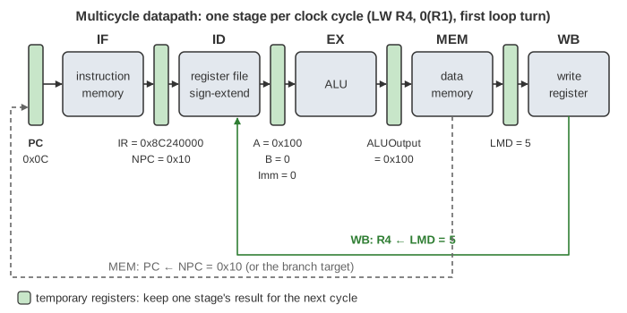
NPC, IR, A, B, Imm, ALUOutput, Cond and LMD are not visible to the program. They hold what one stage produced so that the next stage can use it in the next clock cycle. Because of them, the same hardware can be reused in different cycles: in this design one ALU computes the sum for an ADD, the address for a LW, and the target of a branch. These registers are also the seed of pipelining: in the pipelined MIPS, they become the IF/ID, ID/EX, EX/MEM and MEM/WB pipeline registers. Each of them is a row of edge-triggered D flip-flops: the sequential logic page builds one from gates and shows why it needs a setup time.
The muxes are the control
The four multiplexers choose, for each instruction type, where a value comes from:
- ALU input 1:
A, orNPCfor a branch (to compute the target). - ALU input 2:
Bfor register-register instructions,Immfor everything else. - Next PC:
NPC, orALUOutputwhenCondsays the branch is taken. - Write-back value:
ALUOutput, orLMDfor a load.
A control unit, not drawn in the figure, sets these select lines from the opcode and the current stage. It also tells the register file which register to write (rd for R-format, rt for I-format), whether the data memory reads or writes, and which operation the ALU does.
The muxes, the ALU and the adders are combinational logic: no memory, outputs settling a few gate delays after the inputs change. Combinational Logic builds them from gates and shows the delays and glitches; the clock period must be long enough for them to settle before the next register captures the result.
Instruction formats
R-format  | op 6 | rs 5 | rt 5 | rd 5 | shamt 5 | funct 6 |   ADD SUB AND OR SLT   (op = 0, funct picks the operation)
I-format  | op 6 | rs 5 | rt 5 |      immediate 16         |   ADDI SLTI LW SW BEQZ BNEZ
Example: LW R4, 0(R1) is op 35 (100011), rs 1, rt 4, imm 0: 0x8C240000. The field bar under the datapath splits IR into these fields after every fetch.
The figure's branch unit only tests whether A is zero, so the branches here are BEQZ and BNEZ. They are encoded as the real MIPS32 beq rs, $zero and bne rs, $zero. The branch offset counts instructions from the next one, which is why the target is NPC + (Imm << 2).
A worked example: LW R4, 0(R1)
In the array-sum program, the first time round the loop, with PC = 0x0C and R1 = 0x100:
IF   IR ← Mem[0x0C] = 0x8C240000     NPC ← 0x0C + 4 = 0x10
ID   A ← R1 = 0x100   B ← R4 = 0     Imm ← sign-extend(0x0000) = 0
EX   ALUOutput ← A + Imm = 0x100                     (ALU inputs: A, Imm)
MEM  LMD ← Mem[0x100] = 5            PC ← NPC = 0x10  (PC mux: NPC)
WB   R4 ← LMD = 5                                     (WB mux: LMD)
Cycles per instruction
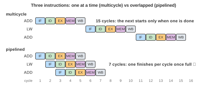
Branches and stores have nothing to write back, so they finish after MEM, in 4 cycles. All the others take 5. The array sum runs 19 instructions (3 set-up, 3 loop turns of 5, 1 store) in 3·5 + 3·(5+5+5+5+4) + 4 = 91 cycles: a CPI of about 4.79. The counters under the data memory keep track.
Most of the hardware sits idle in each cycle: while the ALU works, the instruction memory and the register file wait. Pipelining overlaps the stages: while one instruction is in EX, the next is in ID and the one after it in IF. Ideally that finishes one instruction every cycle (CPI close to 1). Overlapping brings new problems, called hazards: an instruction that needs a register the previous one has not written back yet (data hazards, solved by forwarding and stalls), and a branch whose outcome is known only in MEM while the next instructions are already fetched (control hazards). See them on the MIPS pipeline page, which runs the same programs pipelined.
Try it
- The tabs above the controls load a program at once. One of each goes through every path once: ALU, store, load, a branch taken and one not taken.
- Pick one from the sample instructions list (or type one, such as
sub r5, r3, r1orlw r6, 8(r1)) and press Execute Instruction. It is written into instruction memory at the current PC and run. A branch takes a label from the program or an offset in instructions (bnez r2, -3). - Watch
R0: writes to it are ignored, which is how MIPS gets a constant zero (ADD R3, R0, R0clears R3).
What the animation leaves out
- Only 8 registers, 12 words of instruction memory and 8 words of data memory (0x100–0x11C); the real MIPS has 32 registers and a 32-bit address space.
- Only the instructions the figure can run: no jumps, no
beqbetween two registers, no shifts, multiply or floating point, no exceptions (ADDdoes not trap on overflow). - Real MIPS zero-extends the immediate of
ANDIandORI; the figure has only a sign-extender, so those instructions are left out. - No pipelining, no caches: every memory access takes one cycle. See the CPU cache page for what a real memory access goes through.
References
Classic RISC pipeline (Wikipedia)
Hennessy and Patterson, Computer Architecture: A Quantitative Approach, Appendix C: Pipelining, Basic and Intermediate Concepts (the unpipelined MIPS implementation)