The idea: I/O devices are just addresses
A processor talks to the outside world through I/O devices: LEDs, switches, serial ports, timers, sensors. Each device has a few registers. In a MIPS system the processor reaches them the same way it reaches memory: with lw and sw to reserved addresses. This is memory-mapped I/O. There are no special I/O instructions.
A microcontroller such as the PIC32 (a MIPS core with memory and peripherals on one chip) puts dozens of such devices on the chip. Each tab of the page shows one of them, at the level of registers, wires and clock edges:
| Tab | Device | What to watch |
|---|---|---|
| Memory-mapped I/O | two I/O registers next to RAM | the address decoder, write enables, read mux |
| GPIO | port D: switches in, LEDs out | TRIS, LAT, PORT; polling |
| UART | serial port to a PC terminal | the frame on the wire, baud rate, sampling |
| SPI | serial link to a sensor | two shift registers swapping a byte |
| Timer & Interrupts | Timer1 and two CPUs | polling vs an interrupt service routine |
Memory-mapped I/O and the address decoder
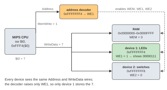
In the book's system, I/O device 1 is at address 0xFFFFFFF4 and I/O device 2 at 0xFFFFFFF8. The processor's Address, WriteData and MemWrite wires go to RAM and to the devices. An address decoder looks at the address and decides who listens:
| Address | sw: write enable | lw: RDsel |
|---|---|---|
RAM (here 0x00000000–0x0000FFFF) | WEM = MemWrite | 00: RAM |
0xFFFFFFF4 | WE1 = MemWrite | 01: device 1 |
0xFFFFFFF8 | WE2 = MemWrite | 10: device 2 |
| anything else | none | none (reads 0 here) |
A store writes only the register whose enable is 1. A load reads all three outputs at once, and the read mux picks one with RDsel. The book's program writes 7 to device 1 and reads device 2:
addi $t0, $0, 7
sw   $t0, 0xFFF4($0)   # device 1 = 7
lw   $t1, 0xFFF8($0)   # $t1 = device 2
The offset 0xFFF4 is only 16 bits. Bit 15 is 1, so sign extension turns it into 0xFFFFFFF4, and $0 as the base gives that exact address. In Demo 1 device 1's LEDs show 00000111, $t1 gets the switches, 0x13, and the same value then goes to and from RAM word 0x40. The timing diagram shows WE1 high only in cycle 2, WEM only in cycle 4, and RDsel = 10 in cycle 3 and 00 in cycle 5.
An address no one decodes fails silently (Demo 2): the store to 0xFFFFFFFC asserts no enable and the value is lost, the load returns 0, and the program gets no error. A real processor would raise a bus error exception. See The Single-Cycle MIPS Processor for where MemWrite and ReadData come from.
GPIO: TRIS, LAT and PORT
General-purpose I/O (GPIO) pins can be inputs or outputs, chosen by software. On the PIC32 each port (A–G) has three main registers. Port D:
| Register | Address | Meaning of bit i |
|---|---|---|
TRISD | 0xBF8860C0 | 1 = pin RDi is an input (reset value), 0 = output |
PORTD | 0xBF8860D0 | reading gives the level on the pin |
LATD | 0xBF8860E0 | the value driven on the pin when it is an output |
The page wires four switches to RD11:8 and four LEDs to RD3:0, and runs:
TRISD = 0xFF00;              // RD15:8 inputs, RD7:0 outputs
while (1) {
    sw = (PORTD >> 8) & 0xF;  // read the switches
    LATD = sw;               // drive the LEDs
}
In C the registers are just variables at fixed addresses, so PORTD compiles to lw and LATD = sw to sw. The book writes PORTD = sw; on the PIC32 a write to PORT writes the latch too.
After reset every pin is an input, so a program that forgets TRISD (Demo 4) writes LATD = 0x0005 but the output drivers stay off: the LEDs are dark, and reading PORTD gives 0x0500, only the switches. The opposite mistake, making a switch pin an output, makes the pin driver fight the switch.
Polling
The loop above is polling: the CPU checks the input again and again. It reacts only when it next reads. In Demo 3 SW1 is flipped right after the read at tick 4, so the write at tick 5 still drives the old value (the timing diagram marks it red), and LED1 turns on only at tick 8, after the next read at tick 7. The worst-case delay is one pass of the loop, and the CPU spends all its time checking, even when nothing changes.
Serial I/O
Sending a byte over 8 parallel wires is fast but needs many pins. Serial I/O sends one bit at a time over one or two wires. Two common kinds: synchronous links send a clock with the data (SPI); asynchronous links send no clock and agree on the speed in advance (UART).
UART: the frame and the baud rate
A UART (universal asynchronous receiver/transmitter) sends each byte as a frame. The line idles at 1. A frame is a start bit (0), the 8 data bits least significant bit first, an optional parity bit, and a stop bit (1). The common format "8N1" means 8 data bits, no parity, 1 stop bit: 10 bits per byte.
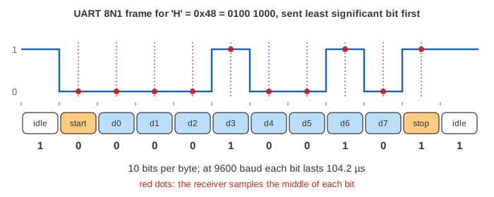
The baud rate is the number of bits per second. At 9600 baud a bit lasts 1/9600 s = 104.2 µs, so 8N1 carries 960 bytes per second. The PIC32 makes its baud rate from the peripheral clock: U1BRG = PBCLK / (16 × baud) − 1; with a 20 MHz clock, U1BRG = 129 gives 9615 baud, 0.16 % off.
The receiver has its own clock. It waits for the falling edge of a start bit, then samples the line in the middle of each bit: half a bit time after the edge for the start bit, then one bit time apart. Real UARTs check the line 16 times per bit, so they find the edge within 1/16 of a bit; the page includes that delay. Sampling in the middle leaves room for small speed differences. In Demo 5 both sides use 9600 baud and "Hi" arrives intact.
| Receiver | 'H' = 0x48 arrives as | Why |
|---|---|---|
| 9600 baud | 0x48 'H' | every sample in the middle of its bit |
| 14400 baud (Demo 6) | 0x20 (space), framing error | samples too often; the "stop bit" sample lands in d5 = 0 |
| 7200 baud | 0xD4, no error flag | samples too slowly; the last ones read the idle line, which looks like a valid stop bit |
A framing error (FERR) means the stop bit was read as 0. The slow case shows that a wrong baud rate does not always raise a flag. As a rule the two clocks must agree within about 2–5 %: over the 10 bits of a frame the sample point may drift less than half a bit.
A parity bit makes the number of 1s even (even parity) or odd. It detects any single flipped bit, but not two. In Demo 7 noise flips d0 on the wire: 'H' = 0x48 (two 1s, parity 0) arrives as 0x49 'I', three 1s plus parity 0 is odd, so the receiver sets PERR.
SPI: two shift registers in a ring
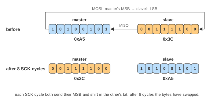
SPI (serial peripheral interface) has a master that drives the clock SCK, and one or more slaves. Data goes out on MOSI (master out, slave in) and comes back on MISO (master in, slave out). Each slave has a chip select (CS, also SS), active low: only the selected slave listens and drives MISO.
Master and slave each hold an 8-bit shift register. On every clock cycle each one sends its MSB and shifts in the other's bit at its LSB. After 8 cycles the bytes have swapped (Demo 8: master 0xA5, slave 0x3C → master 0x3C, slave 0xA5). Every transfer is an exchange: to read a sensor, the master sends a byte, often a dummy one. The colours on the canvas follow each bit from one register to the other.
Two settings must match on both sides. CPOL is the level SCK idles at; CPHA says on which edge data is sampled:
| Mode | CPOL | CPHA | Sample on | Change on | With this mode-0 slave |
|---|---|---|---|---|---|
| 0 | 0 | 0 | rising | falling | master 0x3C, slave 0xA5 |
| 1 | 0 | 1 | falling | rising | slave gets 0xD2: one bit late |
| 2 | 1 | 0 | falling | rising | master gets 0x1E: one bit late |
| 3 | 1 | 1 | rising | falling | works, like mode 0 |
The PIC32 names these bits differently: CKP = CPOL and CKE = NOT CPHA. Try the master mode menu. If CS is never pulled low (Demo 9), the slave ignores the clock and leaves MISO floating; a pull-up makes the master read 0xFF, and the slave's register keeps 0x3C.
SPI is faster and simpler than a UART (no start/stop bits, no agreed baud rate, the clock comes with the data) but needs 4 wires and a separate CS per slave. See Sequential Logic for the flip-flops a shift register is made of.
Timers
A timer is a counter clocked by the peripheral clock through a prescaler. Timer1 on the PIC32 counts in TMR1 and compares it with the period register PR1. When they are equal, TMR1 goes back to 0 and the hardware sets the interrupt flag T1IF in IFS0. The period is (PR1 + 1) timer clocks; here PR1 = 7, so T1IF is set every 8 ticks, at the end of ticks 7, 15, 23 and 31. Timers measure time, make delays, and generate periodic events such as blinking an LED or sampling a sensor.
Interrupts vs polling
The timer tab runs two copies of the same board. Board A polls: its loop does 4 instructions of work, then reads IFS0, tests T1IF and, if set, clears it and toggles the LED. Board B uses an interrupt: its main loop only works. With the interrupt enable bit T1IE = 1, a set flag makes the CPU finish its instruction, save the return address in EPC, and jump to the interrupt service routine (ISR). The ISR clears T1IF, toggles the LED and returns with eret.
| 32 ticks (Demo 10) | Board A (polling) | Board B (interrupt) |
|---|---|---|
| LED toggles | 2 | 3 |
| latency, flag set → LED | 8, 10 ticks | 3, 3, 3 ticks |
| useful work | 16 instructions | 18 instructions |
| timer events lost | 1 (the flag was set again at tick 23 before A cleared it at tick 24) | 0 |
Polling latency depends on where the loop is when the flag is set, and every check costs instructions even when nothing happened. A loop that is too slow even loses events: a flag is only one bit, so a second event before the first is handled leaves no trace. A tighter loop reacts sooner but does less work. The interrupt costs a fixed, short delay (enter, clear, toggle) and nothing at all while no event arrives. Polling is still fine when events are frequent or the CPU has nothing else to do.
The ISR must clear the flag. If it forgets (Demo 11), the flag is still 1 after eret, so the CPU is interrupted again at once: board B toggles its LED 6 times in 32 ticks but only the first toggle answers a real timer event (5 are spurious, 3 events are lost), the main program stops after 7 instructions, and only a reset ends it. This is an interrupt storm. With T1IE = 0 the opposite happens: the flag is set and nothing ever runs. The Interrupt-Driven I/O page shows the same idea from the operating system's side, and DMA how a device moves whole blocks without the CPU.
What the page leaves out
- The single-cycle CPU, the decoder and the devices are drawn as blocks; RAM shows only one word. A real decoder checks address ranges, not single addresses.
- PIC32 details: the real address map (kseg1, physical addresses), the SET / CLR / INV shadow registers (used here by name only), analog pins (ANSEL), open-drain outputs, pull-up configuration.
- The UART's FIFOs, flow control (RTS/CTS), receive interrupts, voltage levels (RS-232, USB bridge) and the 16× majority vote around each sample.
- SPI: one slave only, one byte per transfer, no FIFO, no multi-byte commands; I2C is not shown.
- Interrupts: one source, no priorities or nesting, no vectored vs single-vector modes, no saving of registers in the ISR; one instruction per tick everywhere.
- PWM, analog-to-digital and digital-to-analog conversion (§8.6.6), and other peripherals such as I2C and USB.
See also Virtual Memory in Hardware: in a system with virtual memory, I/O pages are mapped uncached so every lw really reaches the device.
References
Harris and Harris, Digital Design and Computer Architecture, MIPS edition, Sections 8.5: Memory-Mapped I/O and 8.6: Embedded I/O Systems
Microchip, PIC32MX3XX/4XX Family Data Sheet (I/O ports, timers, SPI, UART, interrupts)
Microchip, PIC32 Family Reference Manual, Section 21: UART
Analog Devices, Introduction to SPI Interface (clock polarity and phase)