The idea: a loop of gates remembers a bit
A combinational circuit (an adder, a multiplexer) has outputs that depend only on its inputs right now. A sequential circuit also depends on what happened before: it has state. Registers, counters, the program counter and the pipeline registers of a CPU are all sequential.
The state lives in a feedback loop. Feed the output of a gate back to an input of another gate whose output comes back to the first, and the loop can sit in one of two stable states. That is one bit of memory. The page builds everything else from this loop.
The simulation is gate by gate. Time goes in ticks, and every gate takes exactly one tick to react (a unit delay). Wires are green for 1, grey for 0 and blue for X (unknown); the chip next to each wire says the same in text. A gate whose output changed in the current tick glows orange. The timing diagram under the circuit records every signal over time, like a logic analyser.
The SR latch
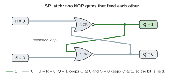
Two NOR gates feed each other: Q = NOR(R, Q̄) and Q̄ = NOR(S, Q). A NOR gives 1 only when both its inputs are 0.
| S | R | Q next | What happens |
|---|---|---|---|
| 0 | 0 | Q | Hold: each gate keeps the other in place. |
| 1 | 0 | 1 | Set: S forces Q̄ to 0 (one tick), then Q rises to 1 (the second tick). |
| 0 | 1 | 0 | Reset: R forces Q to 0, then Q̄ rises. |
| 1 | 1 | Q = Q̄ = 0 | Not allowed: the outputs are no longer opposites. |
After S goes back to 0, Q stays 1. The latch remembers that S was pulsed. (Demo: set and reset, SR latch tab.)
S = R = 1 is forbidden for a second reason. If both are released in the same tick, both gates see 0 0 and both want to switch to 1 at once, then both back to 0, and so on. With perfectly equal gates this would never stop. (Demo: S = R = 1, SR latch tab.)
The gated D latch and transparency
To make the forbidden input impossible, put two AND gates and an inverter in front of the SR latch: S = D · EN and R = D̄ · EN. Now there is one data input D and an enable EN, here driven by the clock.
- While CLK = 1 the latch is open (transparent): Q follows D, three gate delays later.
- While CLK = 0 both AND gates give 0, so S = R = 0 and the latch holds.
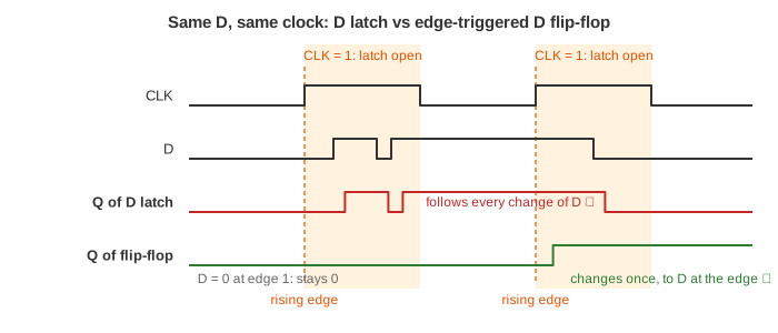
Transparency is the problem. Every change of D while the clock is high goes straight through to Q. In a circuit where the latch's output feeds back, through logic, into its own input (a counter does this), the value would race around the loop many times during one high phase. (Demo: Q follows D, Gated D latch tab.)
The edge-triggered D flip-flop
Put two D latches in a row and give them opposite enables. The master is open while CLK = 0 (it gets CLK̄ through an inverter) and the slave is open while CLK = 1. They are never both open for long, so D cannot run straight through.
- CLK = 0: the master follows D; the slave is closed and holds Q.
- Rising edge: the master closes with the value D had just before the edge, and the slave opens and copies it to Q.
- CLK = 1: the master is closed, so changes of D are ignored until the next edge.
So Q changes only just after a rising edge, to the value of D at that edge. This is a positive-edge-triggered D flip-flop, the building block of every register. Run the same D waveform as demo 3: the latch's Q went up and down during the first high phase, but the flip-flop's Q changes only once, 3 ticks after the second edge. (Demo: only at the edge, D flip-flop tab: the same D as the latch demo.) The slave's R gate reads the master's Q̄m directly, so it needs no second inverter: 10 gates in all.
Setup time, hold time, clock-to-Q
Because the flip-flop is made of gates, it has timing rules. The page measures them on its own gate-level flip-flop (one tick = one gate delay). A NOR latch is a little faster at 0 than at 1, so each number is the worst of the two directions, as in a datasheet:
| Parameter | Meaning | This flip-flop |
|---|---|---|
| tcq clock-to-Q | time from the edge until Q has its new value | 3 ticks (Q rising 3, Q falling 2) |
| tsu setup time | D must be stable this long before the edge, for Q to come at the normal tcq | 4 ticks (D falling 4, D rising 3) |
| th hold time | D must stay stable this long after the edge | 1 tick: D must not change in the edge tick itself |
The amber bar under the D row of the timing diagram marks this window at every edge: D must not change in the 3 ticks before the edge or in the edge tick itself. Demo: setup and hold (D flip-flop tab, period 8, rising edges at 4, 12, 20, …) changes D at different distances from an edge:
- D rises at 8, 4 ticks before the edge at 12: Q rises at 15, 3 ticks after the edge, as it should.
- D falls at 18, 2 ticks before the edge at 20: the master has not settled when the edge comes. Q is still right, but it falls at 24 instead of 22. Real flip-flops do this too: clock-to-Q grows as D gets close to the edge.
- D rises at 28, in the edge tick: the master's enable falls while its inputs are changing. It is left with Qm = Q̄m, which is metastable; Q is X for a few ticks and then settles at random (here to 0). The next edge, at 36, takes D = 1 again.
- D falls at 37, 1 tick after the edge at 36: ignored. Q falls only after the next edge, at 46.
Metastability
A latch whose two gates are left in the same state with nothing driving them is balanced on a knife edge. Real gates are never exactly equal, and noise is always there, so it falls one way or the other. But nobody can say which way, or exactly when. The page draws this as X for 2 to 5 ticks and then picks 0 or 1 at random. (The random numbers come from a fixed seed, so a demo always gives the same result and undo replays it.)
An input that comes from outside the clock domain (a button, another chip with its own clock) can change at any time, so it will sometimes violate setup or hold. Real designs pass such signals through a synchronizer: two flip-flops in a row, so that the first one has a whole clock period to resolve before the second one samples it.
Registers, counters and state machines
A register is a row of flip-flops on the same clock. Add combinational logic that computes the next state from the current state and you have a finite-state machine: at every rising edge, the register loads the next state. The 3-bit counter is the simplest one:
D0 = NOT Q0
D1 = Q1 XOR Q0
D2 = Q2 XOR (Q1 AND Q0)     count: 0 → 1 → 2 → … → 7 → 0
See also Finite State Machines: the same register-plus-logic template with inputs and outputs, as the traffic light controller and Moore and Mealy pattern recognizers, cycle by cycle with binary and one-hot encodings.
Each flip-flop box is the 10-gate circuit of the D flip-flop above, simulated gate by gate. The "master" line inside each box shows its master latch. (Demo: P = 9, 3-bit counter tab.)
Look at D2 after the step 7 → 0: it is 1 for one tick. The XOR sees Q2 fall before the AND output Q1·Q0 falls, so for one tick it computes 0 XOR 1. Such glitches are normal in combinational logic and harmless here: a flip-flop only looks at D around the edge, and the glitch is over long before the next one. The count row shows the same thing: for a tick or two between two states it can show a value in between (3 → 0 → 4), because Q bits that fall switch one tick before Q bits that rise.
The maximum clock frequency
After an edge, the new state has to travel from the flip-flops, through the slowest path of the logic (the critical path), and arrive at a D input before the setup window of the next edge opens. So the clock period must satisfy
Here the critical path is Q → AND → XOR → D2, 2 gate delays, so T ≥ 3 + 2 + 4 = 9 ticks. At P = 9 the counter is right forever (Demo: P = 9).
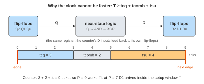
At P = 8 it still counts correctly, but at the step 6 → 7 D2 falls only 3 ticks before the next edge, inside the setup window, and FF2 answers a tick late. Timing analysis would reject P = 8: it works with no margin, and a slightly slower gate (heat, low voltage) would break it. At P = 7 the counter runs once round, then fails at 7 → 0: D2 falls 2 ticks before the edge, FF2's master settles late, and its slave closes (the high phase is only 3 ticks) before the new value has passed through. FF2 goes metastable, and from then on the count is wrong or unknown. (Demo: too fast (P = 7).) At P = 6 it fails already at 1 → 2.
| Clock period P | Counter |
|---|---|
| 12, 9 | 0 1 2 3 4 5 6 7 0 1 … (correct, with margin) |
| 8 | correct, but D2 changes inside the setup window (no margin) |
| 7 | wrong from 7 → 0: FF2 metastable |
| 6 | wrong from 1 → 2 |
A CPU's clock rate is set the same way: by the slowest path between two registers. Pipelining (see the MIPS pipeline) cuts the long path through a whole instruction into five short paths between pipeline registers, so the clock can run faster. The temporary registers of the multicycle MIPS datapath are flip-flops like these. There is also a hold check: the fastest path must not change a D input inside the hold window just after the edge. Here the fastest path (Q → NOT → D0) takes at least 2 + 1 = 3 ticks, far more than th = 1.
Try it
- On the SR latch, toggle S on and off, run a few ticks, then toggle R.
- Open the D flip-flop tab, toggle D just before an edge (look at "next at t =" in the Behaviour panel), and run ticks.
- Open the 3-bit counter tab, run 16 ticks at period 9, then pick period 7 and keep running.
What the page leaves out
- Real gates have analogue delays that depend on load, voltage and temperature. Here every gate takes exactly one tick, and rising and falling are equally fast.
- Real flip-flops are built from transistors and transmission gates (often with an inverter loop and clocked switches), not from NOR gates. The timing rules are the same, but the numbers are much smaller: tens of picoseconds in a modern CPU.
- Clock skew (the clock reaching flip-flops at different times), clock trees, asynchronous set and reset inputs, enable inputs, scan chains and power are not modelled.
- Real metastability resolves after a random time with an exponential tail; the page uses 2 to 5 ticks.
References
Metastability (electronics) (Wikipedia)
Sarah L. Harris and David Harris, Digital Design and Computer Architecture, chapter 3: Sequential Logic Design (latches, flip-flops, finite-state machines, timing of sequential logic)