The idea: every memory is the same array
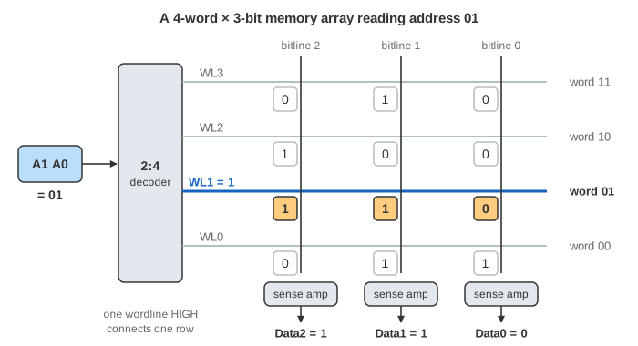
A memory array stores 2N words of M bits. Its depth is the number of words, its width the bits per word. The page uses the book's 4-word × 3-bit array: a 2-bit address A1 A0 and three data bits, Data2 to Data0.
The array is a grid of bit cells, one row per word and one column per bit. An N:2N decoder (the one on the Combinational Logic page) turns the address into exactly one HIGH wordline. That wordline connects its row of cells to the vertical bitlines. Reading senses the bitlines. Writing drives them. The kind of memory is decided only by what sits in each bit cell.
The six tabs show four kinds of cells (DRAM, SRAM, ROM, register file) and two logic arrays that reuse the same grid to compute functions (PLA, FPGA lookup table).
Decoder, wordlines, bitlines
In Demo 1, address 01 makes the decoder raise WL1 only. The three cells of word 01 are connected to their bitlines; the other 9 cells are cut off. At the bottom of each column sits a sense amplifier, which turns a small bitline voltage into a clean 0 or 1, and a write driver, which forces the bitline to the new value.
Real arrays are much wider than one word per row: a row (a DRAM "page") holds thousands of bits, and a column mux picks the word. The page keeps one word per row, as the book does.
DRAM: one transistor and one capacitor
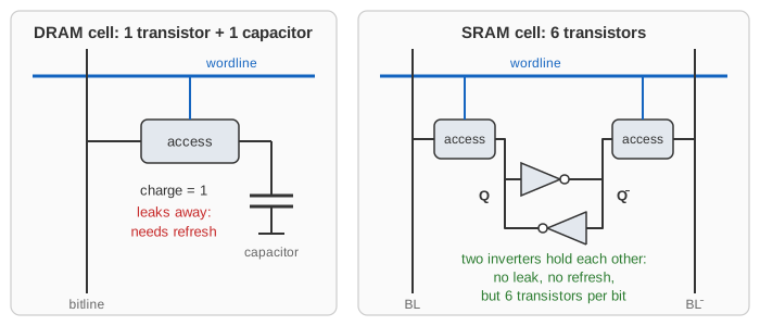
A DRAM cell is an access transistor and a capacitor. The wordline drives the transistor's gate. A charged capacitor is a 1, an empty one a 0. The cell is tiny, so its capacitance is much smaller than the bitline's (1 : 9 on this page). That causes everything else:
- Precharge: before a read the bitlines are set to half of VDD, 0.50 V.
- Charge sharing: when the wordline opens, the cell and the bitline share their charge. A full cell lifts the bitline only to 0.55 V, an empty one pulls it to 0.45 V.
- Sensing: the sense amplifier compares the bitline with 0.50 V and drives it all the way to 1.00 V or 0 V.
- Write-back: the read left the cell at about half charge. The read is destructive, so the amplified value is written back while the wordline is still open.
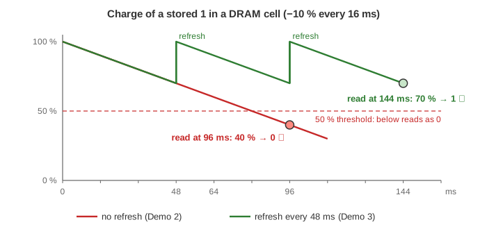
The charge also leaks away through the transistor. On the page a charged cell loses 10 % every 16 ms. A 1 written at t = 0 is at 60 % after 64 ms, which still reads as 1, but at 40 % after 96 ms, which reads as 0. Demo 2 waits 96 ms and then reads word 01: it returns 000, and the write-back makes the loss permanent. All six stored 1s are now lost.
The cure is refresh: read every row and write it back before any 1 falls below the threshold. In Demo 3 the page refreshes every 48 ms. The weakest 1 never drops below 70 %, and word 01 still reads 110 at t = 144 ms. The chart shows the saw-tooth. Real DRAM must refresh every row at least every 64 ms. The memory controller does it in short bursts between normal accesses, so a little bandwidth is lost.
| Demo | What happens to word 01 (110) | Lost bits |
|---|---|---|
| 1: read at t = 0 | bitlines 0.55, 0.55, 0.45 V → 110, written back | 0 |
| 2: read at t = 96 ms, no refresh | 1s at 40 %: bitlines 0.49 V → 000 | 6 |
| 3: refresh at 48 and 96 ms, read at 144 ms | 1s at 70 %: bitlines 0.52 V → 110 | 0 |
SRAM: cross-coupled inverters
An SRAM cell is two cross-coupled inverters, the same loop as the bistable element on the Sequential Logic page, plus two access transistors. Q connects to the bitline BL and the opposite value Q̅ to bitline-bar BL̅. The inverters always drive the cell from VDD, so nothing leaks away and there is no refresh.
To read, both bitlines are precharged HIGH. When the wordline opens, the side that stores 0 pulls its bitline down a little, and a differential sense amplifier sees which of the pair is lower. The read does not disturb the cell. To write, strong drivers force BL = D and BL̅ = not D and overpower the inverters. Demo 4 writes 011 to word 10, reads it, waits 96 ms and reads 011 again.
Area, speed and cost per bit
The cell decides the cost. A big array needs long wordlines and bitlines, so it is also slower. That is why computers use a memory hierarchy: a few fast, costly bits near the processor and many cheap, slow bits behind them.
| Bit cell | Transistors per bit | Cost | Speed | Used for |
|---|---|---|---|---|
| flip-flop | ≈ 20 | very high | fastest | pipeline registers, state |
| register file (2 read + 1 write port) | ≈ 10 | high | fast | the 32 MIPS registers |
| SRAM | 6 | medium | medium | caches |
| DRAM | 1 + a capacitor | low | slow | main memory |
| ROM | 1 or none | lowest | medium | fixed tables, boot code |
Volatile and nonvolatile
DRAM and SRAM are volatile: they forget everything when the power goes. In Demo 5 the SRAM wakes up with arbitrary contents. Each cell falls to whichever inverter happens to be stronger. The page draws the values from a fixed pseudo-random sequence, so the demo always shows the same garbage. A ROM is nonvolatile. It has nothing to forget (Demo 7).
ROM and dot notation
A ROM stores a bit as the presence or absence of a transistor. In dot notation, a dot where a wordline crosses a bitline means a 1. The top row of the book's ROM has a single dot, under Data1, so address 11 holds 010.
On the page every dot is a transistor. The bitlines are weakly pulled HIGH. The raised wordline turns on the transistors of its row, which pull their bitlines LOW, and an inverter under each column turns LOW into 1. (The book's bit cell does it the other way round: a transistor stores a 0 and there is no inverter. Either way the dots show the data.) A mask ROM's transistors are placed when the chip is made, so a write does nothing (Demo 7). PROM, EPROM, EEPROM and flash can be programmed, slowly and a limited number of times.
Logic with a memory array
A 2N-word × M-bit ROM is a lookup table: the address is the input, the word is the output, and each column is one function of N inputs. Reading all four words (Demo 6) fills in the truth table of the book's ROM:
| A1 A0 | Data2 = A1 ⊕ A0 | Data1 = A̅1 + A0 | Data0 = A̅1 · A̅0 |
|---|---|---|---|
| 00 | 0 | 1 | 1 |
| 01 | 1 | 1 | 0 |
| 10 | 1 | 0 | 0 |
| 11 | 0 | 1 | 0 |
Register files and ports
Each port of a memory is one address input with its own data lines. The MIPS register file is a 32-word × 32-bit array with three ports: read ports A1 → RD1 and A2 → RD2, and a write port A3, WD3 with write enable WE3. In one cycle an add rd, rs, rt reads rs and rt and writes rd (Demo 8: RD1 = 5, RD2 = 7, $t2 = 12). This is the register file of the single-cycle MIPS processor.
Each port has its own 5:32 decoder, and every cell gets one wordline and its own bitlines per port, so a register-file cell is larger than an SRAM cell. The reads are combinational. The write happens at the rising clock edge that ends the cycle. So add $t0, $t0, $t0 reads the old value 5 on both ports and writes 10 (Demo 9). Register $0 has no write wordline. It always reads 0, and writes to it are ignored (Demo 10).
Programmable logic arrays
A ROM used as logic spends one row on every one of the 2N input combinations: its decoder is a complete, fixed AND plane. A PLA makes the AND plane programmable too. It builds only the product terms it needs, then ORs them in an OR plane. The book's 3 × 3 × 2 PLA computes X = A̅B̅C + ABC̅ and Y = AB̅ with 3 product terms. The same functions as a ROM need 8 rows (Demos 11 and 12: both always agree; X = 1 only for 001 and 110, Y only for 100 and 101).
FPGAs: lookup tables and logic elements
An FPGA is an array of configurable logic elements (LEs) joined by programmable wiring. Each LE has a lookup table (LUT): 16 SRAM cells and a 16:1 mux whose select lines are the four inputs. In other words, a 16 × 1 memory. Any function of four inputs is just its truth table written into the cells. The LE also has a flip-flop and an output mux that chooses the combinational or the registered value.
The configuration is a bitstream. Loading it writes the LUT cells and the mux settings. In Demo 13 the LUT is programmed for X (1s in cells 2, 3, 12 and 13) and answers 1 for A B C D = 0010. In Demo 14 the same LUT is reprogrammed as 4-input parity, and the output for 1100 changes from 1 to 0 without any rewiring. In Demo 15 the output is registered: Y changes only at a rising clock edge.
| ROM | PLA | FPGA | |
|---|---|---|---|
| AND plane | fixed decoder, all 2N minterms | programmable, only the terms used | none: LUTs hold truth tables |
| Programmed | at manufacture (mask) or once | at manufacture or once | at every power-up (SRAM), any number of times |
| State | no | no | flip-flop in every LE |
What the page leaves out
- The voltages, the 1 : 9 capacitance ratio, the leak of 10 % per 16 ms and the 50 % threshold are illustrative. Real DRAM cells keep their charge far longer than 64 ms. The refresh interval is set by the weakest cells and by temperature.
- One word per row. Real DRAM opens a whole row of thousands of bits into a row buffer, and a column mux picks the word (row hits and misses, banks, burst transfers, the DDR protocol and refresh commands are not shown).
- Transistor-level detail: the access transistor's threshold drop, how a sense amplifier latches, the read-stability and write-margin sizing of the SRAM transistors, and leakage paths.
- Only 8 of the 32 registers are drawn. Pipelined MIPS writes the register file in the first half of the cycle and reads it in the second (see the MIPS Pipeline page). Here the write is at the end of the cycle, as in the single-cycle processor.
- An FPGA's programmable routing, carry chains, block RAMs, DSP blocks and I/O are not drawn. Only one LE is shown.
- Flash, EEPROM, 3D NAND and new nonvolatile memories (MRAM, PCM) are only mentioned.
One level up, DRAM and SRAM become the main memory and caches of the CPU Cache page. On the Levels of Abstraction page, a printf ends up in DRAM cells like these.
References
Harris and Harris, Digital Design and Computer Architecture, Section 5.5: Memory Arrays, and Section 5.6: Logic Arrays
Weste and Harris, CMOS VLSI Design, Chapter 12: Array Subsystems (SRAM, DRAM, ROM, sense amplifiers)
Intel (Altera), Cyclone IV Device Handbook: Logic Elements and Logic Array Blocks