The idea: outputs from inputs, with no memory
A combinational circuit computes its outputs only from the values on its inputs right now. It has no memory and no clock. Give it the same inputs and it gives the same outputs, every time. So a truth table, one row per input combination, describes it completely.
Most of a processor is combinational: the adders, the ALU, the multiplexers that pick operands, the decoders that pick a register. The rest is sequential: registers and memories that hold values from one clock cycle to the next. The MIPS datapath shows both: the boxes PC, IR, A, B and ALUOutput are registers, and everything between them is combinational logic like the circuits on this page.
In the levels of abstraction of a computer, these circuits are the Logic and Digital Circuits levels: below them are voltages and transistors, above them the microarchitecture.
The page builds each circuit from gates and simulates it one gate delay (written τ) at a time. A wire at 1 is dark blue, a wire at 0 is grey. When a gate's inputs change, it gets an orange tag such as →1 @3: its output will become 1 at t = 3 τ. Click an input box on the circuit to flip it, then press Step 1 τ to advance one delay, or Settle to run until nothing is pending. The timing diagram under the explanation records every signal, so you can see how long each output takes and whether it blinks on the way.
Logic gates and truth tables
A gate computes one Boolean function. In hardware a gate is a few transistors; here it is a box that takes one delay to react. Basic gates tab, Demo: all rows.
| Gate | Expression | A B = 00 | 01 | 10 | 11 | In words |
|---|---|---|---|---|---|---|
| AND | A·B | 0 | 0 | 0 | 1 | 1 only if both are 1 |
| OR | A + B | 0 | 1 | 1 | 1 | 1 if either is 1 |
| NOT | A' | 1 | 1 | 0 | 0 | flips A |
| NAND | (A·B)' | 1 | 1 | 1 | 0 | NOT of AND |
| NOR | (A + B)' | 1 | 0 | 0 | 0 | NOT of OR |
| XOR | A ⊕ B | 0 | 1 | 1 | 0 | 1 if A and B differ |
| XNOR | (A ⊕ B)' | 1 | 0 | 0 | 1 | 1 if A and B are equal |
NAND is universal: NOT A = A NAND A, AND = NOT of NAND, and OR = (A NAND A) NAND (B NAND B). So any circuit can be built from NAND gates only. In CMOS a NAND (or NOR) is the cheapest gate, which is why real chips are full of them.
From a truth table to a circuit
Any truth table can be turned into gates. For each row where the output is 1, write an AND of the inputs, with an input inverted when it is 0 in that row. This AND term is a minterm: it is 1 in that row only. OR all these terms together. The result is a sum of products, and it is always correct, though rarely the smallest circuit.
Take the carry-out of a full adder. It is 1 in rows 011, 101, 110 and 111:
Cout = A'·B·Cin + A·B'·Cin + A·B·Cin' + A·B·Cin     (4 three-input ANDs + a 4-input OR)
     = A·B + A·Cin + B·Cin                          (simplified: the "majority" of 3 inputs)
     = A·B + (A ⊕ B)·Cin                             (the form the full adder on the page uses)
A Karnaugh map finds the simplification by eye: it places the rows so that neighbours differ in one input, and each group of neighbouring 1s becomes one shorter term.
| Cout | B Cin = 00 | 01 | 11 | 10 |
|---|---|---|---|---|
| A = 0 | 0 | 0 | 1 | 0 |
| A = 1 | 0 | 1 | 1 | 1 |
The three pairs of 1s (the column B Cin = 11, and the two pairs in row A = 1) are B·Cin, A·Cin and A·B.
Half adder and full adder
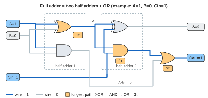
Adding two bits gives a 2-bit result: 1 + 1 = 10 in binary. A half adder computes it with two gates: the sum bit S = A ⊕ B and the carry C = A·B. A full adder also adds a carry coming in from the bit to its right: S = A ⊕ B ⊕ Cin. It is built from two half adders and an OR for the two carries, which is exactly the circuit the page loads first.
Count the delays on the longest path: A changes, the first XOR reacts (1 τ), the AND of the second half adder (2 τ), the OR (3 τ). So the full adder settles in at most 3 τ. Full adder tab, Demo: 1 + 0 + 1 takes that path. On the way, S blinks to 1 at 1 τ and back to 0 at 2 τ, because the second XOR saw Cin = 1 before A ⊕ B had arrived.
Ripple-carry adder and its delay
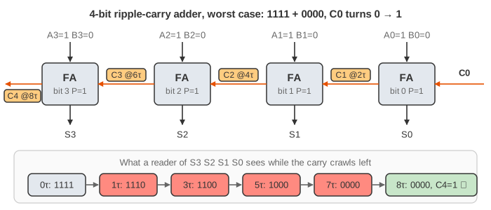
To add two n-bit numbers, chain n full adders: the carry-out of bit i is the carry-in of bit i + 1. This is the ripple-carry adder. It is small, but the carry has to pass through every bit. Each bit adds 2 τ to the carry (an AND and an OR), so the worst case for 4 bits is about 2n + 1 = 9 τ.
Ripple-carry adder tab, Demo: worst case uses A = 1111, B = 0000 and switches C0 from 0 to 1. Every bit propagates the carry (P = A ⊕ B = 1), so the carry crawls one bit every 2 τ. On the way the sum reads 1110, 1100, 1000 and finally 0000 with C4 = 1 at 8 τ. Any circuit that reads the sum before then gets a wrong answer. Demo: no carries settles at 2 τ: the delay depends on the data, but the clock must allow for the worst case.
Faster adders compute the carries in parallel. With generate Gi = Ai·Bi and propagate Pi = Ai ⊕ Bi (both drawn in each FA block), Ci+1 = Gi + Pi·Ci. Expanding this, C2 = G1 + P1G0 + P1P0C0, and so on: two levels of gates for every carry. That is the carry-lookahead adder; it costs more gates, and its delay grows with log n instead of n.
See also Arithmetic Circuits: a 16-bit carry-lookahead adder and a prefix adder raced against ripple carry with gate delays, plus subtraction, comparators, a barrel shifter and an array multiplier.
Signed overflow
The same adder adds signed numbers in two's complement: 1111 is −1, 1000 is −8, 0111 is +7. The result is wrong only when it does not fit in 4 bits, and that happens exactly when the carry into the sign bit differs from the carry out of it: V = C3 ⊕ C4. Demo: 7 + 1 overflow adds 0111 + 0001: the sum 1000 is 8 unsigned (fine, C4 = 0) but −8 signed (wrong), and V = 1. In the worst-case demo, V blinks: C3 arrives 2 τ before C4, so the XOR sees them differ for a moment.
See also Number Systems: Two's Complement, Fixed Point and IEEE 754: the same carry-out vs overflow rule on 8-bit words, negation, sign extension, fixed point, and how floating-point numbers are encoded and added.
Multiplexers and decoders
A multiplexer (mux) chooses: the select input S picks which data input reaches the output. A 2:1 mux is F = A·S' + B·S. A 4:1 mux uses two select bits and four AND terms. In the MIPS datapath every choice is a mux: ALUSrc (register or immediate), MemtoReg (ALU result or loaded word), the next PC (PC + 4 or the branch target).
A decoder turns an n-bit number into 2n lines, exactly one of them 1. Each output is one minterm of the address bits. Decoders pick the register to write in a register file, the memory chip to enable, and the control signals for an opcode. Decoder tab, Demo: one line on shows E = 1 with address 10 turning on D2 only.
See also Memory Arrays, where a 2:4 decoder raises one wordline of a DRAM, SRAM or ROM array, and a ROM or PLA computes logic functions.
Propagation delay, the critical path and the clock
A gate's output changes some time after its inputs: its propagation delay. A circuit's outputs are only correct after the change has passed through the longest chain of gates between any input and any output, the critical path. Until then the outputs can hold old values, half-updated values, or short pulses.
This is what limits the clock. A register at the start of the logic launches new values at a clock edge; a register at the end must not capture them before they settle. So the clock period must be longer than the critical path delay (plus the registers' own setup time and clock-to-output delay). A 4-bit ripple adder with 9 τ is fine; a 64-bit one with 129 τ is not, which is why real ALUs use lookahead adders.
Glitches (hazards)
When two paths from the same input reach a gate with different delays, the output can briefly take a wrong value even though the correct value before and after is the same. This is a glitch, and the condition that allows it is a hazard.
Multiplexer tab, Demo: glitch holds A = B = 1, so F should stay 1 whatever S is. When S goes from 1 to 0, the term B·S drops at 1 τ, but S' needs one gate (the NOT) before A·S' can rise at 2 τ. For one delay both terms are 0, and F drops to 0 at 2 τ and returns at 3 τ: a static-1 hazard.
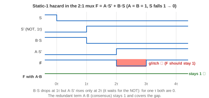
The fix is a redundant term: A·B is 1 whenever A and B are both 1, independent of S, and covers the gap (Demo: glitch removed, or tick consensus term A·B on the Multiplexer tab). On a Karnaugh map it is the group that joins the two others; the theorem behind it is the consensus theorem, A·S' + B·S = A·S' + B·S + A·B. The decoder has the same problem: when the address changes, D0 can blink because A1' arrives one delay after A1.
In a clocked processor glitches inside the logic do no harm, because registers sample only after the outputs have settled. They matter where a signal is used without a clock: clocks themselves, asynchronous resets, write enables of memories, and power (every blink charges a wire).
The ALU
The 4-bit ALU is the one from Patterson and Hennessy, made of four 1-bit ALU slices. Each slice has an AND gate, an OR gate, a full adder (the box marked +, built from gates inside) and a 4:1 mux that picks the result with the 2-bit Operation. In front of the inputs, two 2:1 muxes can invert a and b (Ainvert, Bnegate). The carry ripples from slice 0 to slice 3.
| ALU control (Ainvert Bnegate Op) | Function | How |
|---|---|---|
| 0000 | AND | mux input 0 |
| 0001 | OR | mux input 1 |
| 0010 | add | mux input 2, the adder |
| 0110 | subtract | a + b' + 1: Bnegate inverts b and is also CarryIn of bit 0 |
| 0111 | set on less than (slt) | subtract; bit 3's sum (the sign of a − b) goes out as Set into Less of bit 0; Less of the other bits is 0 |
| 1100 | NOR | a'·b' = (a + b)' by De Morgan, mux input 0 |
Zero is a NOR of the four result bits; the branch beq uses it after a subtraction. Overflow is C3 ⊕ C4 as above. The control lines run to every slice; the page draws them as short labelled stubs (Ainv, Bneg, Op) instead of long wires, as schematics often do.
4-bit ALU tab, Demo: 5 − 3 and slt subtracts 0101 − 0011 = 0010, then sets the op to slt: 5 < 3 is false, so the result is 0000 and Zero = 1. With A = 0011, B = 0101 the result is 0001. Subtract and slt are the slowest operations, up to 14 τ here: Bnegate first passes an inverter and a mux, the carry then ripples through all four bits, and for slt the sign of bit 3 must still travel back to bit 0's result mux, with Zero after that.
Try it
- Pick a circuit with the tabs at the top. It loads with all inputs at 0, settled. Each tab shows only the controls that circuit uses.
- Click an input box (0 / 1) on the circuit to flip it. Or type values in the inputs field (
A=0111 B=0001 C0=0; a value with several digits sets bits 3..0) and press Set Inputs. - Press Step 1 τ repeatedly and watch the orange tags: those gates change next. Press Settle to finish.
- Changing an input while the circuit is settled restarts the clock at t = 0. Changing it while changes are still pending keeps the clock running, as in real hardware.
- The Multiplexer tab has the consensus term checkbox; the 4-bit ALU tab has the ALU op select, which applies as soon as you pick an operation.
- The Demo buttons of each tab play a prepared sequence; Undo steps back through it.
Combinational logic plus a state register makes a finite state machine: see Finite State Machines, where the next-state and output equations are evaluated every clock cycle.
What the page leaves out
- Real delays differ. Every gate here takes 1 τ and every mux 2 τ. In CMOS an XOR is slower than a NAND, a gate with more inputs is slower, and the delay grows with the number of gates a wire drives (fan-out) and the wire length.
- Inertial delay. The simulation uses transport delay, so every pulse passes through. Real gates swallow pulses shorter than their own delay, so some glitches never appear.
- Transistors and voltages. A 1 is a voltage range, rising and falling take time, and there are no undefined (X) or high-impedance (Z) values here.
- Faster arithmetic. Carry-lookahead, carry-select and prefix adders, multipliers and dividers.
- Sequential logic. Latches, flip-flops, registers and the clock that samples settled outputs. See the MIPS datapath and the MIPS pipeline.
References
Patterson and Hennessy, Computer Organization and Design, Appendix A (The Basics of Logic Design): gates, decoders, multiplexers, the 1-bit and 32-bit ALU, carry lookahead
Harris and Harris, Digital Design and Computer Architecture, chapter 2 (Combinational Logic Design): Karnaugh maps, timing, glitches